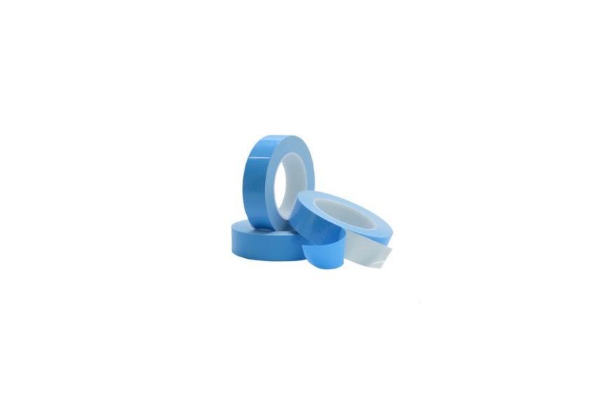
Welcome to Taxo Tape
How to Select the Right Thermal Pad for Solar Inverter Applications
The Thermal Problem Inside a Solar Inverter
Solar inverters don't get much credit for how hard they work thermally. The conversation around inverter design tends to focus on conversion efficiency, MPPT accuracy, grid compliance — the electrical performance metrics that show up in product brochures. Thermal management sits further down the list, and TIM selection often happens last, almost as a procurement detail rather than an engineering decision.
That sequencing creates problems. The thermal interface material occupies the most thermally critical position in the entire heat dissipation stack: the bond line between the power device and whatever is removing its heat. At that interface, a poorly matched pad doesn't fail dramatically — it just underperforms quietly. Junction temperatures run a few degrees higher than the simulation predicted. Efficiency degrades slightly at high ambient temperatures. After two or three years of daily thermal cycling, what was marginal at commissioning has drifted into a reliability problem.
This article is aimed at engineers and procurement managers specifying thermal pads for solar inverter designs — string inverters, central inverters, hybrid storage inverters, and the power conversion stages inside them. It covers the parameters that genuinely drive selection, the tradeoffs that aren't obvious from datasheets alone, and the specification mistakes that appear repeatedly in inverter designs that come back with thermal complaints.

What Makes Solar Inverter Thermal Environments Demanding
Understanding why inverters are a particularly challenging application for thermal interface materials starts with the operating environment — which is more punishing than most indoor industrial equipment.
Ambient temperature range is wide, and the extremes are real. A rooftop or ground-mount installation in a temperate climate routinely sees ambient temperatures from below −20°C in winter to above 45°C on a summer afternoon — sometimes on the same installation site. Coastal and desert deployments push those limits further. The thermal pad has to function across that entire range: maintain adequate contact at cold-start when the material is at its stiffest, and sustain performance when the enclosure interior temperature is well above 60°C under peak solar irradiance and full load.
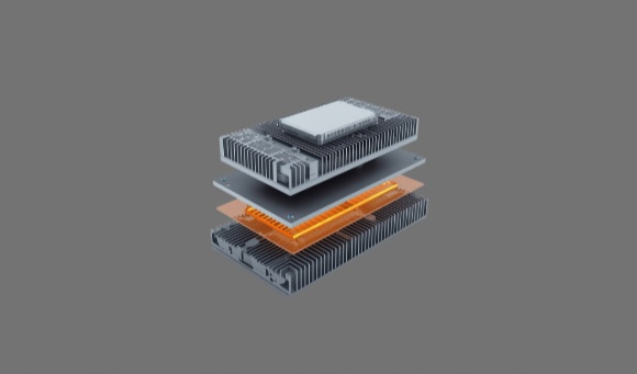
Power density has increased, enclosure size has not. Modern string inverters pack 5 kW to 15 kW or more into enclosures not much larger than a residential electrical panel. IGBT switching losses, diode reverse-recovery losses, and inductor copper losses all generate heat in a tightly confined volume. IP55 or IP66-rated enclosures — standard for outdoor installations — restrict natural convection significantly. Many designs route heat conductively from power components through a thermal pad to the enclosure back panel, which acts as a passive heatsink exposed to ambient air. That thermal path runs entirely through solid materials, and the pad is the highest-resistance element in it.
Grid-tied inverters run long hours without scheduled downtime. Unlike industrial drives or UPS systems that cycle with process demand, a solar inverter tracks available irradiance from sunrise to sunset, every day, for a design life measured in decades. The cumulative thermal cycling exposure — thousands of daily heat-up and cool-down cycles over a 20-year service life — is substantial. Each cycle stresses the interface mechanically: the power device, the thermal pad, and the heatsink all have different coefficients of thermal expansion, and they expand and contract at different rates. A pad that maintains good contact in year one needs to still be doing its job in year ten.
Field service is expensive. Unlike equipment in a factory or data center, a malfunctioning inverter on a rooftop or in a ground-mount array requires a site visit to diagnose and repair. Thermal failures that develop gradually — rising junction temperatures, increased thermal resistance at the interface due to pad degradation — don't trigger obvious fault codes. They manifest as reduced output at high temperatures, occasional over-temperature shutdowns, or shortened device life. By the time the failure is traced to the TIM interface, the cost of the service visit often exceeds the cost of the inverter's entire thermal management bill of materials. Getting the pad selection right at the design stage is considerably cheaper than correcting it in the field.
The Parameters That Actually Drive Selection
Thermal pad datasheets present a consistent set of parameters, but not all of them carry equal weight in an inverter application. Some numbers that look important are less predictive of real-world performance than they appear; others that are easy to overlook often determine whether a design succeeds or fails in service.
3.1 Thermal Conductivity — Necessary but Insufficient
Thermal conductivity is the number printed largest on every thermal pad product page, and it's the starting point for any selection. For inverter-grade thermal pads, the practical range runs from roughly 3 W/m·K for general-purpose silicone pads up to 8–10 W/m·K for high-performance boron nitride-filled grades. Some specialty products exceed that, but they come with tradeoffs in cost, hardness, or processability that aren't always justified.
The problem with leading the selection process with conductivity is that it's a bulk material property measured in isolation. It tells you how heat moves through the pad itself, not how effectively heat transfers across the interface between your specific component surface and your specific heatsink. That interface performance depends on contact area, which is a function of surface roughness, pad hardness, and clamping pressure — none of which appear in the conductivity figure.
Two pads with identical thermal conductivity ratings but different hardness and surface texture can deliver meaningfully different interface thermal resistance values in the same assembly. The conductivity number is necessary for comparison; it's not sufficient for selection.
3.2 Interface Thermal Resistance
Interface thermal resistance — typically reported in units of °C·cm²/W or K·cm²/W — is a more useful predictor of real-world performance because it captures both the bulk conductivity and the contact behavior at the interface. It's the metric that directly translates into junction temperature in your thermal model.
Reading datasheet values correctly requires attention to the test conditions under which they were measured. Most manufacturers report interface thermal resistance at a specific applied pressure — commonly 10 psi (69 kPa) or 50 psi (345 kPa) — and at a specific bond line thickness. A pad measured at 50 psi will show considerably better numbers than the same pad measured at 10 psi. If your assembly applies 15 psi at the interface, the 50 psi datasheet value is not the number to use in your thermal budget.
For IGBT module interfaces in inverter designs, practical interface thermal resistance targets typically fall in the range of 0.1 to 0.5 °C·cm²/W, depending on the power dissipation and the allowable temperature rise across the interface. Smaller driver components and gate resistors are less sensitive — interface resistance in the 0.5 to 1.5 °C·cm²/W range is usually acceptable there. Knowing these targets before you evaluate datasheets keeps the selection process grounded in what the application actually requires rather than chasing the lowest published number.
3.3 Operating Temperature Range
Most thermal pad datasheets list operating temperature ranges that look generous — "−40°C to 200°C" is common. That figure describes the temperature range within which the material doesn't chemically degrade or mechanically fail catastrophically. It says nothing about how thermal resistance or mechanical compliance varies across that range, which matters considerably in an inverter application.
Silicone elastomers stiffen at low temperatures. A pad that compresses easily at room temperature becomes harder to conform at −20°C — the cold-start condition for an inverter in a northern climate. Clamping force that was adequate for good contact at assembly temperature may not be sufficient to maintain contact when the pad is at its stiffest. This is worth verifying with the material supplier, particularly for designs where cold-start thermal performance is part of the functional specification.
At the high end, the distinction between a pad's sustained operating rating and its short-term peak rating matters. An inverter running at full rated power on a 45°C ambient day, inside an IP66 enclosure with limited airflow, can expose the TIM interface to temperatures well above 100°C. The pad needs to perform continuously at that temperature, not just survive it briefly. Confirm the sustained rating — not the maximum rating — against your worst-case thermal analysis.
3.4 Hardness and Compression Behavior
Hardness determines how much clamping force is required to achieve adequate surface contact, and how the pad behaves mechanically over years of service.
Softer pads — Shore OO 30 to 50, for reference — conform to surface irregularities under lower applied pressure, which is useful in assemblies where clamping force is limited by component lead or solder joint strength. The tradeoff is susceptibility to compression set and cold flow under sustained mechanical load. Over years of continuous compression in a hot enclosure, a very soft pad can permanently deform, reducing its effective thickness and potentially changing its contact behavior at the interface.
Harder pads resist pump-out and cold flow more effectively but require greater clamping force to achieve equivalent conformability. For large IGBT module interfaces with controlled bolt torque, this is manageable. For smaller components attached with spring clips or low-torque fasteners, it becomes a constraint.
Compression set — the permanent deformation retained after sustained compression — is a parameter that rarely receives enough attention during initial selection. A pad specified for a 20-year inverter service life should be evaluated on compression set data, not just initial hardness. Ask the supplier for compression set figures at the relevant temperature and time conditions; if that data isn't available, treat it as a gap in your selection basis.
3.5 Electrical Insulation
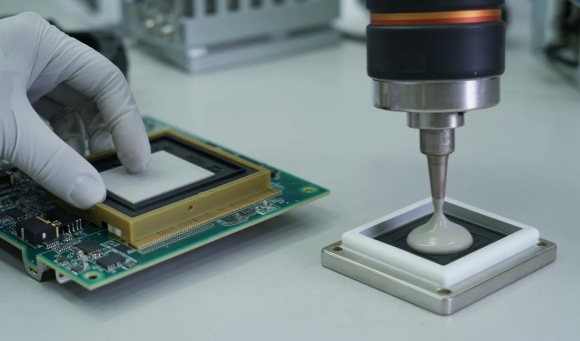
Many inverter thermal paths cross an electrical isolation boundary. The IGBT module baseplate may carry switching voltage; the heatsink or enclosure back panel is chassis-grounded. In that configuration, the thermal pad must simultaneously conduct heat and block current — a dual requirement that significantly narrows the material options.
Boron nitride-filled silicone pads are the standard solution for this application. BN is an electrically insulating ceramic with thermal conductivity significantly higher than aluminum oxide, making it possible to achieve both properties in a single material. Dielectric strength for BN-filled pads typically falls in the range of 8 to 15 kV/mm, depending on pad thickness and specific formulation. Aluminum oxide-filled pads offer lower conductivity at similar thickness but can also provide adequate insulation for lower-voltage isolation requirements.
One detail that's easy to overlook: dielectric strength scales with thickness, but not linearly. A thicker pad doesn't simply multiply the thin-pad dielectric strength value. Verify the dielectric strength at your actual specified thickness — suppliers should be able to provide this data for standard product grades.
3.6 Outgassing and Environmental Stability
Standard silicone thermal pads contain volatile siloxane compounds that can outgas slowly at elevated temperatures. In an open or well-ventilated environment, this is rarely a concern. In an IP65 or IP66 sealed inverter enclosure, it can be.
Siloxane vapor that accumulates inside a sealed enclosure can deposit on electrical contacts — relay contacts, connector pins, current sensor optics — forming an insulating film that increases contact resistance or interferes with optical measurement. The failure mode is insidious: contact resistance increases gradually, the connection becomes intermittent, and the root cause is difficult to identify without specifically testing for siloxane contamination.
Low-volatility thermal pad grades — specifically formulated to minimize outgassing at elevated temperatures — are the appropriate choice for sealed enclosure designs. The conductivity and mechanical properties are generally comparable to standard grades; the formulation difference is in the silicone base and curing chemistry. If your inverter design uses sealed enclosures with relays, current sensors, or precision connectors inside, specifying a low-volatility pad is a straightforward precaution that costs little at the material level and can prevent a difficult field failure.
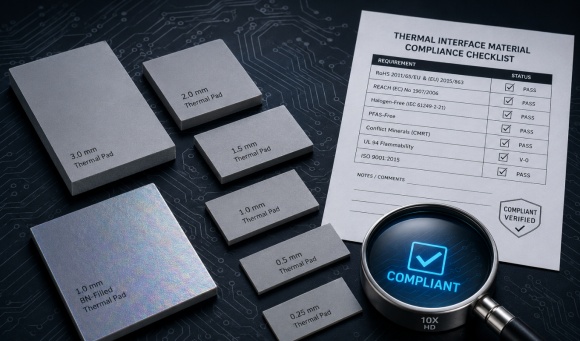
UL 94 flame retardancy is a related consideration. Many inverter system certifications require flame-retardant materials throughout the assembly. Verify that the pad grade you're specifying carries the relevant UL 94 rating — V-0 for most applications — before it reaches a certification audit. Retrofitting a flame-retardant material after the design is locked is an avoidable delay.
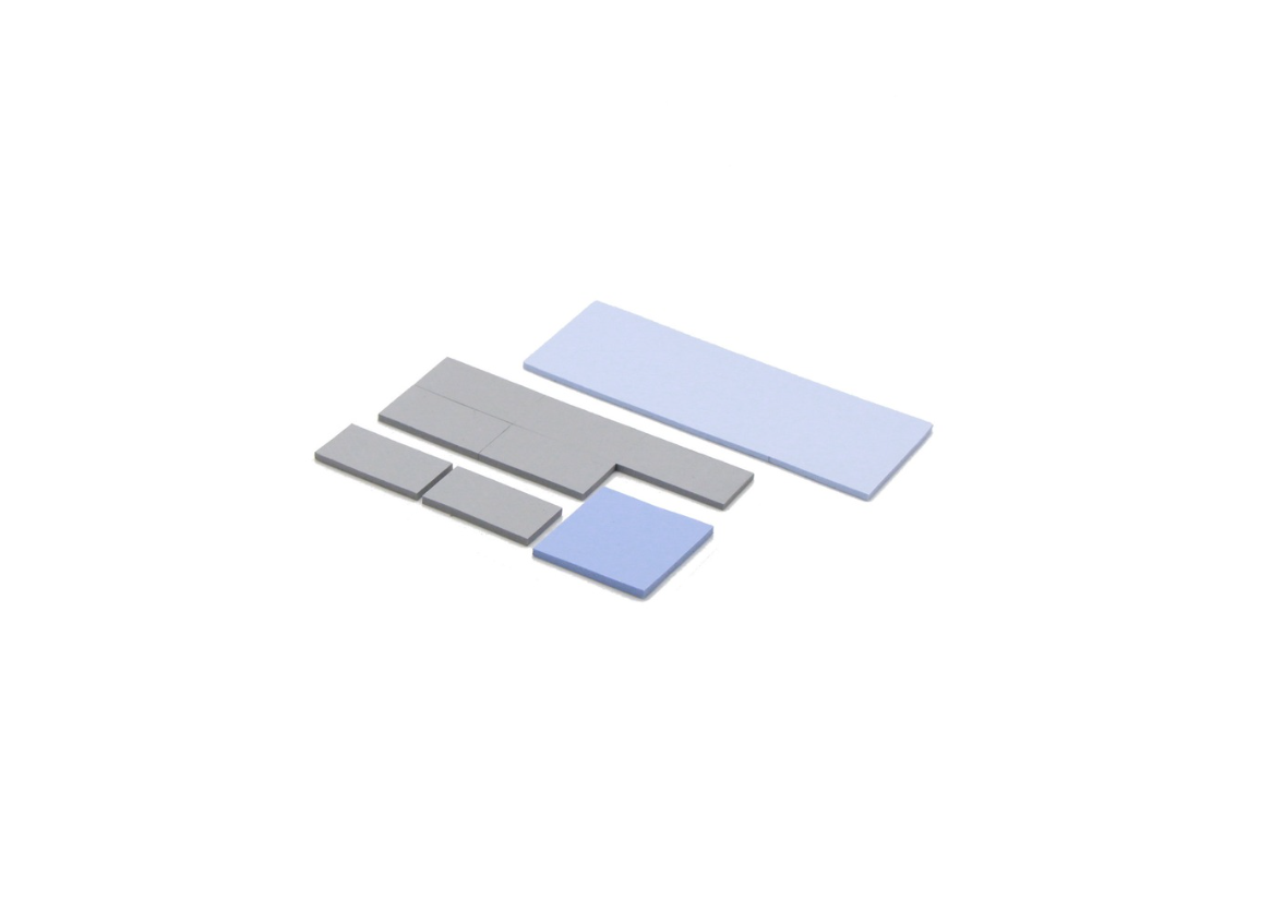
Gap Tolerance and Mechanical Fit
Thermal conductivity and interface resistance get most of the attention in TIM selection discussions. Gap management gets considerably less — and that's where a lot of inverter designs run into trouble.
The gap between a power component's top surface and the heatsink or enclosure wall it's pressing against is rarely a single fixed number in a real assembly. It's a range, determined by the tolerance stack of every part in that mechanical path: component body height, PCB thickness variation, heatsink flatness, mounting boss height, fastener torque variation. For a typical inverter power stage with multiple components on a single heatsink plate, the actual gap can vary by 0.5 mm or more across the board — and that variation exists within a single unit, not just across a production batch.
A thermal pad specified to the nominal gap dimension will be undersized at the tight end of the tolerance range and undersized in contact pressure at the loose end. Neither condition is acceptable for a design intended to run for 20 years.
The practical approach is to specify pad thickness to the upper end of the gap range, then verify that the pad's compression behavior at the lower end doesn't generate excessive stress on component leads, solder joints, or the PCB itself. Soft pads with high compressibility can absorb significant tolerance variation without transmitting damaging force to the component. Harder pads require tighter gap control or a more conservative thickness selection to avoid over-compression.
Mixed-height component populations create a related problem. An IGBT module standing 4 mm above the PCB surface and a gate driver IC standing 2 mm above it cannot both be adequately contacted by a single pad thickness — not without compromising one or the other. The standard solutions are either dedicated pad cutouts of different thicknesses placed at each component location, or a soft, high-compressibility pad grade that accommodates the full height variation across its compression range. Neither approach is perfect; both require deliberate design rather than a single blanket specification.
Surface finish matters more than most procurement processes acknowledge. A machined aluminum heatsink extrusion has a different surface roughness profile than a die-cast aluminum enclosure back panel. Rougher surfaces require a softer, more conformable pad to achieve equivalent contact area at the same clamping force. If your heatsink supplier changes their machining process or casting source mid-production, it can affect thermal interface performance even if the pad specification hasn't changed. This is worth flagging as a process control point, particularly for designs where thermal margins are tight.
Common Specification Mistakes
These aren't hypothetical failure modes. They're patterns that appear repeatedly in inverter designs that come back with thermal complaints, field failures, or certification issues — often traceable to decisions made early in the procurement process that seemed reasonable at the time.
Selecting on thermal conductivity alone. The catalog sort by highest W/m·K, pick the top result, done. The problem is that a high-conductivity pad with inappropriate hardness for the assembly's clamping force — or measured under test conditions that don't reflect the actual application — can deliver worse interface performance than a lower-rated pad that's properly matched to the mechanical design. Conductivity is the starting filter, not the selection criterion.
Ignoring compression set over the product's service life. Initial thermal testing passes. Qualification testing passes. Eighteen months into field deployment, over-temperature events start appearing in inverter logs in high-ambient installations. Investigation eventually traces it to increased thermal resistance at the TIM interface — the pad has taken a permanent set under sustained compression at elevated temperature, reducing effective contact pressure. Compression set data is available from suppliers; it's rarely requested. For a 20-year design life claim, it should be part of the standard evaluation.
Skipping the outgassing check for sealed enclosures. A standard silicone pad is specified because it's familiar, available, and meets the conductivity requirement. The inverter uses an IP66 enclosure with an internal relay for grid connection switching. Two years into service, relay contact resistance has increased enough to cause intermittent dropout events. The failure mode takes months to diagnose. Low-volatility pad grades are not significantly more expensive than standard grades; the specification decision is a minor line item. The field failure it prevents is not.
Using one pad thickness across the entire board. A single 2 mm pad is applied across a power stage with components ranging from 1.5 mm to 3.5 mm in height above the PCB surface. The tallest components are adequately contacted; the shorter ones are not. Thermal imaging at rated load shows hot spots on the shorter components that the thermal simulation — which assumed uniform contact — didn't predict. Fixing this in production requires a pad layout redesign that should have been addressed during prototyping.
Overlooking dielectric requirements until late in the design. The heatsink design is finalized with the thermal pad spec based on conductivity and thickness. During electrical safety testing, it's identified that the pad formulation selected — aluminum oxide-filled, standard grade — doesn't meet the required dielectric withstand voltage for the isolation boundary it's crossing. The heatsink design accommodated a specific pad thickness; switching to a BN-filled grade with different thickness options requires mechanical redesign. Identifying the isolation requirement at the beginning of pad selection costs nothing. Addressing it after the heatsink is tooled is expensive.
A Practical Selection Checklist
Before finalizing a thermal pad specification for a solar inverter design, work through these questions. Most thermal issues that appear in field deployments can be traced to one or more of them being answered incompletely at the design stage.

This isn't a pass/fail checklist — it's a set of questions that should have confirmed answers before a pad is locked into a bill of materials. If several of them are still open when the design enters prototyping, that's the point to resolve them, not after thermal performance data comes back from the first build.
Sample Before You Commit
Datasheets give you a starting point. They don't give you a result.
The only reliable way to validate a thermal pad selection for a specific inverter design is to measure bond-line temperature rise in your actual assembly — your heatsink surface, your component geometry, your fastener torque, your thermal load — under representative operating conditions. That measurement, compared against your thermal model, tells you whether the pad is performing as expected or whether the interface is adding more resistance than the simulation predicted.
A structured sample evaluation doesn't need to be complex. Instrument the device junction and heatsink surface, run the assembly at rated load in your worst-case ambient condition, and record the temperature differential across the interface at steady state. Then repeat after an accelerated thermal cycling sequence — enough cycles to surface any compression set or contact degradation that would otherwise take months to appear in the field. The investment in that evaluation is small relative to the cost of a field thermal issue in a deployed inverter fleet.
Inverter power classes also vary enough that what works well in one design may not transfer directly to another. A thermal pad selection optimized for a 5 kW residential string inverter — modest power density, relatively simple mechanical layout — may not be appropriate for a 100 kW central inverter with higher current densities, larger IGBT module footprints, and more complex heatsink geometry. Treat each design as its own selection exercise rather than carrying a preferred pad specification from project to project without re-evaluation.
If you're working through pad selection for a specific inverter design and want to discuss the application parameters — power dissipation, gap range, enclosure type, isolation requirements — we're glad to help identify materials worth evaluating. Share the details, and we can narrow the field to a short list of candidates for sampling.