Welcome to Taxo Tape
Silicone Thermal Pads: How They Work and How to Select the Right Grade
Introduction
Silicone thermal pads are one of the most widely specified TIMs in power electronics — and also one of the most frequently misspecified. The selection is rarely as simple as picking a pad with the highest conductivity number and the right dimensions. Bond line thickness, compression behavior, electrical insulation grade, and long-term compression set all affect whether the material actually performs as intended in a real assembly.
This article covers the physical mechanisms behind thermal pad performance, the material parameters that matter most for engineering decisions, and a practical framework for matching pad grade to application requirements — whether you're specifying for an industrial inverter, a UPS module, an LED driver assembly, or an EV charging system.
The Physics Behind Thermal Pad Performance
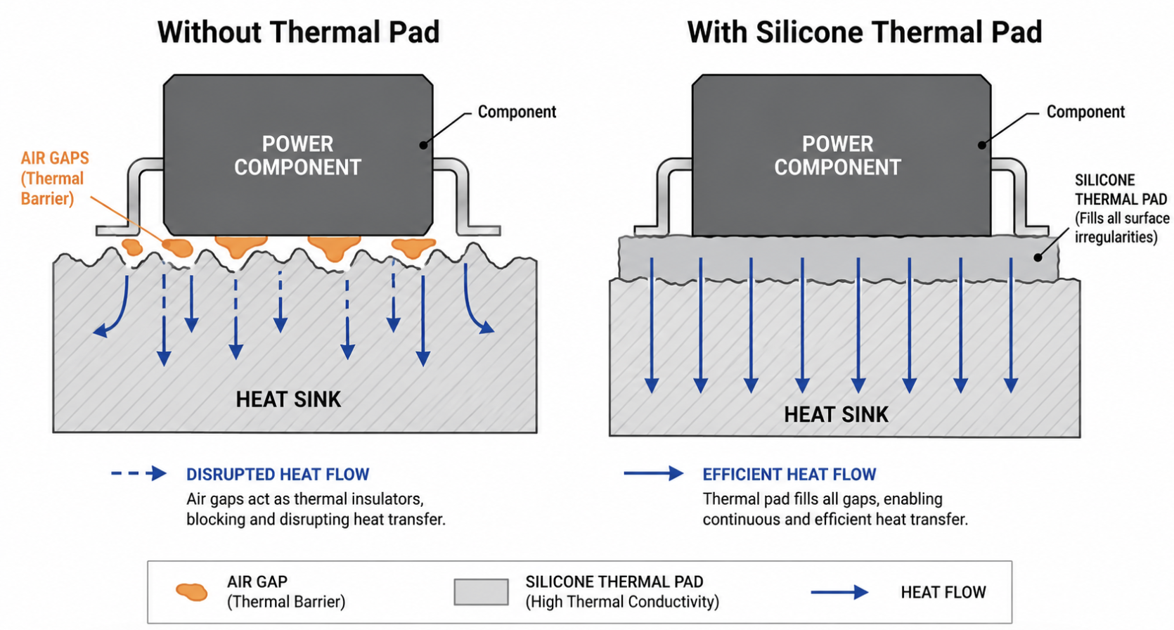
Even surfaces that look flat under normal inspection are not flat at the microscopic level. Machined aluminum heat sinks, PCB surfaces, and power module bases all have surface roughness — peaks and valleys on the scale of micrometers — that prevent full metal-to-metal contact when two components are pressed together.
The result is an interface filled with microscopic air pockets. Air has a thermal conductivity of approximately 0.026 W/m·K — roughly two orders of magnitude lower than aluminum. Even a small amount of trapped air at the interface creates a significant thermal resistance barrier, limiting how efficiently heat can move from the component into the heat sink.
A silicone thermal pad solves this by compressing under mounting pressure and flowing slightly into the surface irregularities, displacing air and creating a continuous, thermally conductive path across the interface. The heat flow path becomes: component surface → pad → heat sink, with the pad's bulk conductivity and compressed thickness determining the thermal resistance contributed by the TIM layer.
The key equation governing this:
R_interface = thickness (m) ÷ conductivity (W/m·K) × contact area (m²)
This means thermal resistance decreases when bond line thickness decreases OR when conductivity increases. Both variables matter — which is why a thinner pad at moderate conductivity can outperform a thicker pad at higher conductivity in the same application.
Material Composition and What It Means for Performance
Base matrix: silicone rubber
The silicone rubber base gives the pad its compliance and temperature stability. Silicone remains flexible and elastic across a wide temperature range — typically -40°C to 200°C for most commercial grades — without hardening, cracking, or losing its gap-filling ability over time. This temperature stability is one of the primary reasons silicone-based pads dominate in power electronics over non-silicone alternatives in most applications.
Thermally conductive fillers
The silicone base alone has a thermal conductivity of roughly 0.2 W/m·K — far too low for thermal management. Thermally conductive filler particles are dispersed through the matrix to increase bulk conductivity. The filler type and loading level determine the pad's position in the conductivity range:
Aluminum oxide (Al₂O₃): Most common filler for standard-grade pads (1–3 W/m·K range). Cost-effective, electrically insulating, widely available.
Zinc oxide (ZnO): Sometimes used in combination with Al₂O₃; similar conductivity range.
Boron nitride (BN): Enables higher conductivity grades (4–10+ W/m·K) while maintaining excellent electrical insulation. Higher material cost.
Graphite or carbon-based fillers: Used in specialty high-conductivity grades; may reduce or eliminate electrical insulation properties depending on formulation.
Higher filler loading increases conductivity but also increases hardness — which is why high-conductivity pads tend to be stiffer and require higher mounting pressure to achieve full contact.
Electrical insulation
The electrical insulation properties of a silicone thermal pad derive from both the silicone matrix and the insulating filler particles. Most Al₂O₃ and BN-filled grades are electrically insulating with dielectric strength typically in the range of 8–25 kV/mm, depending on formulation and thickness. This allows thermal pads to serve dual function — thermal interface and electrical isolator — in high-voltage applications such as IGBT modules and power supply assemblies.
Key Technical Parameters
Thermal conductivity (W/m·K)
Commercial silicone thermal pad grades typically span 1–15 W/m·K, with the majority of industrial power electronics applications covered by the 1–8 W/m·K range:
1–3 W/m·K: Standard grades for moderate heat flux applications — LED driver boards, control electronics, auxiliary power components
3–6 W/m·K: Mid-range grades for IGBT modules, UPS components, industrial inverter boards
6–10+ W/m·K: High-performance grades for high-power-density applications — EV charger power stages, high-current power modules
Higher conductivity is not always better if it comes with increased hardness and reduced compression at your available clamping force.
Thickness and compression rate
Pad thickness should be selected to match the design gap — the space between component surface and heat sink under assembled conditions. Standard commercial thicknesses run from 0.3 mm to 5 mm, with compression rates typically 10–40% under standard mounting pressure.
A common selection error is specifying pad thickness equal to the nominal gap without accounting for surface variation and compression. The correct approach: select a pad thickness slightly above maximum gap tolerance, verify it compresses to within the design gap range under your actual clamping force.
Hardness (Shore 00)
Silicone thermal pads are typically characterized by Shore 00 hardness in the range of 25–60. Softer pads (Shore 00 25–35) conform more readily to surface irregularities under lower clamping force — useful when mounting pressure is limited or surface flatness is poor. Harder pads (Shore 00 45–60) maintain dimensional stability under sustained load — useful in applications with precise gap control requirements or high compression set resistance needs.
Thermal resistance (°C·cm²/W)
Thermal resistance is a more directly useful metric than bulk conductivity for comparing pads in a real application, as it accounts for the specific thickness being used:
R = thickness ÷ conductivity
A 1 mm pad at 3 W/m·K has a bulk thermal resistance of 0.33 °C·cm²/W. A 2 mm pad at 6 W/m·K has the same value. Request thermal resistance data from suppliers at your actual compressed thickness, not at nominal thickness — the difference matters.
Operating temperature range
Standard silicone thermal pads operate reliably from -40°C to 180–200°C depending on formulation. Confirm the upper limit for your specific application — particularly in power electronics where component surface temperatures may exceed 100°C continuously.
Head-to-Head: Silicone Thermal Pad vs. Other TIMs
| Parameter | Silicone Thermal Pad | Thermal Grease | Phase Change Material | Gap Filler |
|---|---|---|---|---|
| Thermal conductivity | 1–15 W/m·K | 3–12+ W/m·K | 3–8 W/m·K | 1–4 W/m·K |
| Bond line thickness | 0.3–5 mm | 20–150 µm | 20–80 µm | 0.5–10 mm |
| Electrical insulation | Built-in (most grades) | Grade dependent | Usually requires separate layer | Grade dependent |
| Gap accommodation | Good | Tight gaps only | Tight gaps only | Excellent |
| Assembly method | Manual placement | Dispense/manual | Peel-and-place | Dispense |
| Pump-out risk | None | Medium–high | None | None |
| Long-term stability | High | Moderate–low | High | High |
| Reworkability | Easy | Difficult | Moderate | Moderate |
| Relative cost | Lower–moderate | Lower | Higher | Moderate |
When silicone pads are the better choice over grease: when the gap exceeds 0.3 mm, when electrical insulation is needed without a separate layer, or when production assembly needs to be fast, clean, and repeatable without dispensing equipment.
When grease or PCM outperforms pads: when the interface is very flat and tight (below 0.1 mm gap) and maximum conductivity with minimum bond line thickness is the primary objective. At those geometries, grease and PCM achieve lower thermal resistance than a compressed pad.
When gap fillers are needed instead of pads: when gap size exceeds 2–3 mm, or when component height variation across the board is too large for a standard pad to bridge reliably. Gap fillers accommodate geometries that pads cannot.
How to Select the Right Grade for Your Application
Step 1: Determine your heat flux and required thermal resistance.
Start with the thermal budget — how much temperature rise across the TIM layer is acceptable given your component's junction temperature limit and your heat sink performance. Work backward from that to the maximum allowable interface thermal resistance, then identify which combination of conductivity and thickness meets it.
For moderate heat flux applications below 5 W/cm² — LED driver boards, control electronics, auxiliary power components — standard grades at 1–3 W/m·K typically provide sufficient performance. For higher heat flux applications — IGBT modules, high-current power stages, EV charger power electronics — grades at 4–8 W/m·K with controlled bond line thickness are more appropriate.
Step 2: Match thickness to your gap geometry.
Measure or model the actual gap under assembled conditions, accounting for surface variation and component height tolerance. Select a pad thickness that compresses to within your target bond line range under your available clamping force. If gap variation across the assembly is significant — more than 0.3–0.5 mm between components — consider whether a softer, more compressible grade or a gap filler is more appropriate than a standard pad.
Step 3: Confirm electrical insulation requirements.
If the TIM sits between a component case and a grounded heat sink at elevated voltage — IGBT modules, power modules, high-side switch positions — confirm the pad's dielectric strength meets your isolation requirement. Standard Al₂O₃-filled grades typically provide 8–15 kV/mm; BN-filled grades can reach 15–25 kV/mm. Specify the minimum dielectric strength required, not just "electrically insulating."
Step 4: Verify compression set for your service life target.
Compression set is the percentage of original thickness a pad loses permanently after sustained compression over time. A pad with high compression set will gradually thin under module clamping load, increasing bond line thickness and thermal resistance over the product's service life. For applications with 8–10+ year design life targets — industrial inverters, UPS systems, EV charging infrastructure — request compression set data from your supplier at your operating temperature and clamping conditions.
Step 5: Decide on format — sheet stock or custom die-cut.
For prototype and low-volume production, sheet stock cut to size is the practical choice. For medium to high-volume production, custom die-cut pads matched to component footprint reduce assembly time, eliminate cutting variability, and improve placement accuracy. The unit cost premium for die-cutting is typically justified at volumes above a few hundred units per month.
Common Selection and Application Mistakes
Selecting grade based on conductivity number alone.
Thermal conductivity tells you the material's bulk heat transfer capability — it doesn't tell you the thermal resistance at your specific thickness under your specific clamping force. Two pads with the same conductivity but different hardness and compression behavior will produce different thermal resistance values in the same assembly. Always evaluate thermal resistance at compressed thickness, not bulk conductivity at nominal thickness.
Specifying thickness equal to nominal gap without accounting for variation.
If your design gap is 1 mm nominal with ±0.3 mm tolerance, a 1 mm pad may bottom out or leave gaps depending on which components are assembled. Specify pad thickness above maximum gap tolerance and verify compression behavior across the full tolerance range.
Ignoring surface preparation.
A thermal pad compressing against a contaminated or oxide-covered surface cannot achieve the interface contact its specification assumes. In production, ensure contact surfaces are clean and free of machining oils, oxides, and particulate contamination before pad placement. This is particularly relevant for aluminum heat sinks, which oxidize readily.
Overlooking compression set in long-life applications.
Compression set data is not always prominently featured in supplier datasheets, but it directly affects thermal performance stability over product lifetime. For any application with a multi-year service life target under sustained clamping load, request compression set data at operating temperature before finalizing grade selection.
TaxoTape® Solutions
TaxoTape® supplies silicone thermal pads across a range of conductivity grades for industrial power electronics applications — from standard Al₂O₃-filled grades for moderate heat flux applications to BN-filled high-performance grades for demanding power module and EV charging applications.
Available in sheet stock and custom die-cut formats matched to component dimensions. Full technical documentation — including TDS, dielectric strength data, compression characteristics, and RoHS declaration — is provided with sample and production orders.
If you are specifying thermal pads for a new design or evaluating alternatives to your current grade, we can recommend specific options based on your gap geometry, heat flux, electrical insulation requirements, and production volume.
Request samples or technical consultation →
Conclusion
Silicone thermal pads solve a real engineering problem — they eliminate the air gaps that limit heat flow at component interfaces — but their performance in a given application depends heavily on whether the right grade is matched to the actual assembly conditions.
Conductivity grade, thickness, hardness, electrical insulation level, and compression set behavior all interact to determine whether a pad meets the thermal and reliability requirements of a specific design. Treating pad selection as a commodity decision — picking any available grade at the right thickness — is where most specification errors originate.
The selection process is straightforward once the thermal budget, gap geometry, insulation requirements, and service life target are clearly defined. Where any of those parameters are uncertain, validating with samples under representative assembly conditions before production commitment remains the lowest-risk path to a reliable design.
Contact TaxoTape® to discuss thermal pad selection for your application →
FAQ
Q: What is the difference between a thermal pad and a gap filler?
Both fill interface gaps and improve thermal contact, but they serve different gap size ranges. Thermal pads are pre-formed solid sheets, typically 0.3–5 mm thick, suited for controlled gap sizes within that range. Gap fillers are dispensable materials — gel or paste form — that accommodate larger or more variable gaps, up to 10 mm or more, and conform to complex surface geometries that a rigid pad cannot. If your gap exceeds 3–4 mm or varies significantly across the assembly, a gap filler is more appropriate than a pad.
Q: Can I reuse a silicone thermal pad after disassembly?
In many cases yes, if the pad remains undamaged, clean, and retains adequate thickness after removal. For prototype and development work, reuse is generally acceptable. For production assemblies and critical applications, replacing with a new pad is recommended — a pad that has been compressed and released may not re-conform as effectively to the interface, particularly if it has experienced partial compression set. Confirm with your supplier whether the specific grade is rated for reuse.
Q: How do I know if my thermal pad is under enough clamping pressure?
Insufficient clamping pressure is one of the most common causes of poor thermal pad performance in production. The pad needs enough force to compress to its target bond line thickness across the full contact area. Most suppliers specify a recommended pressure range — typically 40–200 psi (0.3–1.4 MPa) depending on grade hardness. If thermal performance measurements are higher than expected, verify actual clamping force against the pad specification before investigating other causes.
Q: Is a higher Shore hardness number always worse for thermal performance?
Not necessarily. Softer pads conform more easily to surface irregularities under lower clamping force, which can reduce contact resistance. But harder pads maintain more consistent thickness under sustained clamping load — they resist compression set better over time. The right hardness depends on your surface flatness, available clamping force, and service life requirements. Neither extreme is universally better; match hardness to your assembly conditions.