Welcome to Taxo Tape
High-Conductivity Thermal Pads: When 6+ W/m·K Actually Matters
Introduction
High-conductivity thermal pads carry a meaningful price premium over standard grades — often 40–80% higher per unit area depending on filler system and supplier. That premium is easy to justify when the application genuinely needs it. It is money spent with no measurable benefit when it does not.
The default engineering instinct is understandable: higher W/m·K sounds like better thermal performance, and better thermal performance sounds like lower risk. But thermal resistance in a real assembly depends on more than the pad's bulk conductivity, and past a certain point, increasing conductivity further stops producing any meaningful reduction in junction temperature — because other resistances in the thermal path have become the limiting factor.
This guide works through when high-conductivity pads (typically defined as 6.0 W/m·K and above) actually move the needle on thermal performance, and when a standard mid-range pad delivers the same practical result at meaningfully lower cost. It is written for engineers and procurement teams specifying thermal interface materials for industrial power electronics — inverters, UPS systems, motor drives, and high-power LED and EV charging applications.
What "High Conductivity" Actually Means
Commercial thermal pads fall into rough tiers based on filler system and loading:
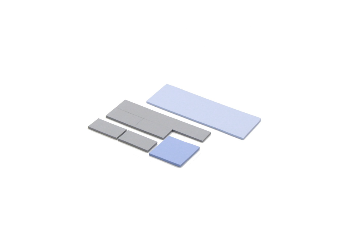
1.0–3.0 W/m·K: standard alumina-filled pads, the default for low-to-moderate dissipation components
3.0–6.0 W/m·K: mid-range alumina or hybrid-filled pads, covering most general industrial power electronics
6.0–10.0 W/m·K: high-conductivity tier, typically achieved through boron nitride (BN) filling or high-loading hybrid formulations
10.0 W/m·K and above: specialized products with significant cost premiums and sometimes mechanical trade-offs
The jump from mid-range to the high-conductivity tier is not simply "more of the same filler." Alumina particles are roughly spherical and pack efficiently up to a point, after which further loading increases hardness and brittleness without proportional conductivity gains. Boron nitride has a platelet crystal structure that conducts heat efficiently along its basal plane, allowing formulators to reach 6–10+ W/m·K while maintaining electrical insulation — a combination that pure metallic fillers cannot offer, since metal particles loaded heavily enough to reach comparable conductivity would compromise dielectric strength.
This is why BN-filled pads dominate the high-conductivity tier in power electronics specifically: the application usually requires both high thermal conductivity and electrical isolation simultaneously, and BN is one of the few filler systems that delivers both at once.
The Diminishing Returns Problem
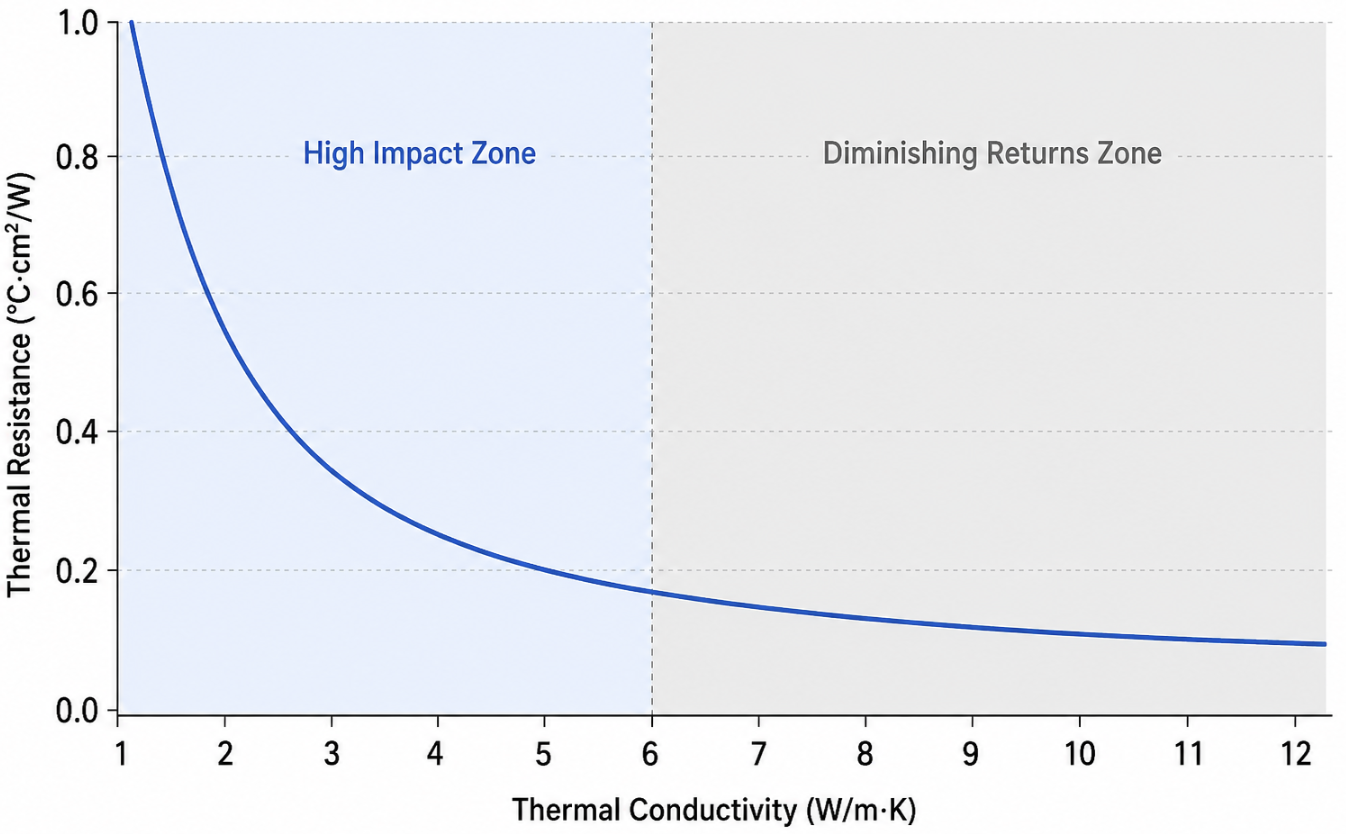
Thermal resistance through a pad follows a simple relationship: resistance decreases as conductivity increases, but not linearly in terms of practical benefit — because the pad is only one contributor to total system thermal resistance.
The math that matters:
Consider a pad at 1.0mm thickness. Moving from 1.0 to 3.0 W/m·K reduces the pad's contribution to thermal resistance from roughly 1.0 °C·cm²/W to 0.33 °C·cm²/W — a reduction of 0.67 °C·cm²/W. Moving from 8.0 to 10.0 W/m·K reduces resistance from 0.125 to 0.10 °C·cm²/W — a reduction of only 0.025 °C·cm²/W. The first upgrade delivers roughly 27 times the resistance reduction of the second, despite both representing a 2.0 W/m·K improvement.
Why this matters for your total thermal budget:
The pad's thermal resistance is only one term in the full thermal path from junction to ambient. That path typically includes junction-to-case resistance (fixed by the device package), the TIM layer, and heat sink-to-ambient resistance (fixed by heat sink design and airflow). If the heat sink and package resistances together account for 80% of your total thermal budget, then even eliminating the pad's resistance entirely only improves total system performance by a fraction of the remaining 20%.
A practical check before specifying high conductivity:
Calculate your full thermal stack resistance using datasheet or simulation values for junction-to-case and heat sink-to-ambient resistance. If the pad's contribution — even at standard 3–6 W/m·K conductivity — represents less than 10–15% of the total budget, upgrading to a high-conductivity grade will produce a junction temperature improvement small enough that it rarely justifies the cost premium. If the pad represents 25% or more of the total resistance budget, the upgrade has real, measurable value.
When High-Conductivity Pads Are Actually Necessary
High heat flux at the primary interface.
Applications generating heat flux above 15–20 W/cm² at the component-to-heat-sink interface genuinely benefit from high-conductivity pads. At these flux levels, even small reductions in interface thermal resistance translate to measurable junction temperature differences — often several degrees per W/m·K improvement at this end of the conductivity range.
IGBT, SiC, and GaN power devices.
Wide-bandgap semiconductors operate at higher power densities and often tighter junction temperature margins than equivalent silicon devices. SiC and GaN devices in particular are frequently specified with thermal budgets that leave little room for interface resistance beyond what a high-conductivity pad provides. In these applications, 8.0–12.0 W/m·K grades are commonly the correct specification, not an over-engineered choice.
Compact designs with limited heat sink area.
When heat sink surface area is constrained by enclosure size — common in compact inverters, dense power supply designs, and space-limited EV charging equipment — the heat sink-to-ambient resistance is higher than it would be with a larger heat sink. This shifts more of the total thermal budget's weight onto the interface, making pad conductivity a proportionally larger factor in total system performance.
Applications requiring both high conductivity and electrical isolation simultaneously.
When the design requires dielectric isolation at the same interface where high thermal performance is needed — a common combination in IGBT modules operating at 600V+ bus voltage — BN-filled high-conductivity pads solve both requirements in a single material. Attempting to achieve equivalent conductivity with a lower-cost filler system that lacks adequate dielectric strength is not a viable substitution in these applications.
When Standard Pads Are the Better Choice
The majority of general industrial power electronics.
Standard mid-range pads at 3.0–6.0 W/m·K cover the thermal requirements of most UPS modules, standard LED drivers, DC-DC converter stages, and moderate-power motor drives without requiring premium material. For these applications, the thermal stack calculation typically shows the pad's contribution is not the limiting factor, and a conductivity upgrade produces negligible practical benefit.
Cost-sensitive production at volume.
The 40–80% price premium for high-conductivity grades compounds meaningfully across production volume. For applications where the thermal calculation does not justify the upgrade, this premium is avoidable cost with no corresponding reliability or performance benefit — a straightforward case for standard-grade specification.
Assemblies with limited clamping pressure.
This is a mechanical trade-off that is easy to overlook. High-conductivity BN-filled pads tend to be firmer than alumina-filled equivalents at comparable hardness ratings, due to the platelet particle geometry affecting compression behavior. In assemblies with limited fastener torque, clip-mounted components, or flexible substrates that cannot apply high clamping force, a high-conductivity pad may fail to achieve full surface contact — producing worse real-world thermal resistance than a softer, standard-conductivity pad that conforms properly under the available pressure. In this scenario, the "better" material on paper underperforms in practice.
Applications where heat sink or package resistance dominates the thermal budget.
As covered in Section 3, if your thermal stack calculation shows the pad represents a small fraction of total system resistance, no pad — regardless of conductivity — will meaningfully change junction temperature. The correct engineering response in this case is to address the heat sink design or component package selection, not to upgrade the TIM.
Head-to-Head: Standard vs. High-Conductivity Pads
| Parameter | Standard Pad (1.0–6.0 W/m·K) | High-Conductivity Pad (6.0–10.0+ W/m·K) |
|---|---|---|
| Typical filler | Alumina (Al₂O₃) | Boron nitride (BN), hybrid BN/alumina |
| Thermal conductivity | 1.0–6.0 W/m·K | 6.0–10.0+ W/m·K |
| Dielectric strength | 8–15 kV/mm | 15–25 kV/mm |
| Hardness/compressibility | Generally softer, conforms at lower pressure | Firmer, requires higher clamping pressure |
| Required assembly pressure | 50–150 kPa typical | 100–250 kPa typical |
| Surface finish tolerance | Forgiving | Less forgiving |
| Relative cost | Baseline | 40–80% premium |
| Best-fit heat flux | Below 10–15 W/cm² | Above 15–20 W/cm² |
| Best-fit devices | Standard MOSFETs, diodes, driver ICs | IGBT, SiC, GaN, high-current modules |
| Value when heat sink resistance dominates | High — cost-effective | Low — premium wasted |
Reading this table for your specification decision:
The conductivity numbers are the most visible difference, but the assembly pressure requirement is the one most likely to cause unexpected performance problems. A high-conductivity pad specified into an assembly with insufficient clamping force will underperform its datasheet value — sometimes significantly — because it cannot achieve full surface contact. Before specifying a high-conductivity grade, confirm your assembly can actually deliver the pressure the material needs.
How to Verify You Actually Need High Conductivity
Step 1: Calculate your full thermal stack.
Gather junction-to-case resistance from the component datasheet, heat sink-to-ambient resistance from the heat sink specification or thermal simulation, and estimate the TIM resistance at your target BLT using standard-grade conductivity (assume 4.0 W/m·K as a baseline). Sum these to get total system thermal resistance, then calculate what fraction the TIM contributes.
Step 2: Apply the 15–20% threshold.
If the TIM's contribution is below 15% of the total budget, a high-conductivity upgrade will produce a junction temperature improvement of only a few tenths of a degree — rarely worth the cost premium. If the TIM's contribution exceeds 20–25% of the total, upgrading conductivity has a meaningful, calculable effect on junction temperature and the premium is justified.
Step 3: Request ASTM D5470 data, not laser flash values.
When comparing high-conductivity products across suppliers, confirm the test method. ASTM D5470 measures thermal impedance under realistic interface pressure and produces values that translate directly to your application. Laser flash diffusivity measures bulk material conductivity in isolation and can produce inflated numbers relative to actual interface performance — this discrepancy is more common at the high-conductivity tier than at standard grades, where datasheet inflation has less commercial incentive.
Step 4: Confirm your assembly pressure meets the material's requirement.
Request the compression stress versus thickness curve for any high-conductivity pad under consideration. Compare this against your actual fastener torque or clamping force. If your assembly applies 80 kPa and the pad's curve shows it needs 150 kPa to reach its rated BLT, the datasheet conductivity value will not translate to your real interface resistance.
Common Mistakes
Specifying the highest available conductivity by default.
Without running the thermal stack calculation in Section 7, "highest conductivity available" is not a specification decision — it is a guess that happens to cost more. Run the calculation before defaulting to premium material.
Ignoring the assembly pressure requirement of high-conductivity grades.
BN-filled pads generally require higher clamping force to achieve full contact than alumina-filled equivalents at comparable hardness. Specifying a high-conductivity pad into a low-pressure assembly — clip-mounted components, thin sheet metal enclosures, limited fastener torque — frequently produces worse real-world performance than a standard-grade pad that conforms properly under the available pressure.
Comparing conductivity values without checking the test method.
A supplier reporting 10.0 W/m·K via laser flash and another reporting 8.0 W/m·K via ASTM D5470 are not offering comparable products. The second may deliver lower actual interface resistance despite the lower headline number. Always confirm the test standard before making a supplier comparison based on conductivity alone.
Treating the TIM upgrade as a substitute for heat sink design improvement.
When thermal simulation shows the heat sink-to-ambient resistance is the dominant term in the thermal budget, no pad conductivity upgrade will meaningfully reduce junction temperature. In these cases, the correct engineering response is heat sink area, fin design, or airflow improvement — not TIM specification. Spending on a premium pad in this scenario produces cost without benefit.
TaxoTape® Solutions
TaxoTape® supplies both standard alumina-filled thermal pads (1.0–6.0 W/m·K) and high-conductivity BN-filled grades (6.0–12.0 W/m·K) for industrial power electronics applications, including IGBT modules, SiC and GaN power devices, and high-power inverter and motor drive assemblies.
All products are supplied with ASTM D5470 thermal resistance test data and compression stress versus thickness curves, allowing you to verify actual interface performance under your specific clamping conditions before committing to production. We can help calculate whether your application's thermal stack justifies a high-conductivity specification, or whether a standard-grade pad delivers equivalent practical performance at lower cost.
Request samples or a thermal stack consultation →
Conclusion
High-conductivity thermal pads are the correct specification for a specific set of conditions: high heat flux at the primary interface, IGBT/SiC/GaN devices with tight junction temperature margins, compact designs with limited heat sink area, or applications requiring simultaneous high conductivity and dielectric isolation. In these cases, the cost premium is justified by a measurable, calculable improvement in junction temperature.
Outside those conditions — the majority of standard industrial power electronics applications — a mid-range pad at 3.0–6.0 W/m·K typically delivers equivalent practical thermal performance, because the pad's resistance is not the limiting factor in the total thermal budget. Paying a 40–80% premium for conductivity that the system cannot use is a common and avoidable cost.
The decision comes down to one calculation: what fraction of your total thermal resistance budget does the TIM actually represent? Run that number before specifying, and confirm your assembly can deliver the clamping pressure a high-conductivity grade requires before assuming the upgrade will perform as its datasheet suggests.
Contact TaxoTape® to calculate whether your application needs high-conductivity thermal pads →
FAQ
Q: How do I estimate my thermal stack resistance without running a full simulation?
Start with the component datasheet's junction-to-case thermal resistance value — this is standard information provided by semiconductor manufacturers. For heat sink-to-ambient resistance, most heat sink suppliers provide this value for their standard products at specified airflow conditions, or it can be estimated from heat sink area and airflow using published correlations. Combined with an assumed TIM resistance at standard conductivity, this gives a reasonable first-pass estimate sufficient for the 15–20% threshold check, even without detailed thermal simulation software.
Q: If my application is borderline — the pad represents about 18% of the thermal budget — should I upgrade?
At the borderline, the decision depends on your margin requirements and cost sensitivity. If your junction temperature has little margin to the device's maximum rating, or if field reliability at the margin is a concern, the upgrade is a reasonable precaution even at 18%. If your application has comfortable thermal margin already, the standard grade is likely sufficient. Running the actual numbers with real component and heat sink data — rather than working from the rough 15–20% rule of thumb — gives a more precise answer for borderline cases.
Q: Can I mix a high-conductivity pad with a smaller heat sink to save space without losing performance?
Not directly, because the pad and the heat sink address different terms in the thermal resistance equation. A high-conductivity pad reduces TIM resistance, but heat sink-to-ambient resistance depends on heat sink surface area and airflow, which the pad cannot compensate for. If you reduce heat sink size, you increase heat sink resistance — a high-conductivity pad will reduce the TIM's contribution but cannot offset an undersized heat sink. Run the combined thermal stack calculation for the proposed smaller heat sink before assuming a pad upgrade compensates for reduced heat sink area.
Q: Does a high-conductivity pad make sense if my device has very low power dissipation but I want extra thermal margin for reliability?
Generally no. If actual heat flux is low, the pad's resistance contribution to the total thermal budget will also be low regardless of conductivity, meaning a high-conductivity grade provides negligible additional margin. Thermal margin in low-dissipation applications is more effectively improved by addressing whichever resistance term is actually largest in your stack — often the heat sink-to-ambient term — rather than upgrading a TIM that is not the limiting factor.