Welcome to Taxo Tape
TIM Selection for LED Chip-on-Board and High-Power LED Packages
Introduction
The thermal interface between an LED package and its heat sink is a different engineering problem than the thermal interfaces inside an LED driver circuit. The LED package operates at a single, concentrated heat source with a tightly defined junction-to-case thermal resistance specified by the manufacturer. The driver circuit, by contrast, distributes heat across multiple discrete components — MOSFETs, capacitors, inductors — each with different thermal requirements and interface geometries.
This distinction matters because TIM selection guidance written for driver circuits does not translate directly to LED chip-level interfaces. A COB (Chip-on-Board) LED array or a high-power discrete LED package has its own set of thermal path characteristics, contact geometry constraints, and reliability considerations that require separate evaluation.
This guide focuses specifically on TIM selection at the LED package-to-heat-sink interface — the thermal path from the LED chip itself, not the driver electronics that power it.
The LED Thermal Path: From Junction to Heat Sink
Why junction temperature is the governing constraint.
LED performance and lifetime are both directly tied to junction temperature — the temperature at the semiconductor die itself, not the ambient or even the case temperature. As junction temperature rises, luminous efficacy decreases (more of the input power converts to heat rather than light), color output can shift, and the rate of lumen depreciation over time accelerates. Most LED manufacturers publish L70 or L90 lifetime ratings — the operating hours until light output degrades to 70% or 90% of initial value — as a direct function of junction temperature, with the ratings dropping substantially as junction temperature increases within the specified operating range.
The thermal resistance chain.
Heat generated at the LED junction must pass through several series resistances before reaching ambient: junction-to-case resistance (fixed by the LED package design, published by the manufacturer as a datasheet parameter), the TIM layer between the LED package and the heat sink or MCPCB, and heat sink-to-ambient resistance (determined by heat sink design and airflow conditions).
The TIM layer is the one link in this chain that the system designer directly controls at the assembly stage. Junction-to-case resistance is fixed by the LED package you have selected — you cannot change it without changing the LED itself. Heat sink-to-ambient resistance is a mechanical design decision made largely independent of TIM selection. The TIM interface is where thermal engineering choices at the assembly level have the most direct, immediately controllable impact on final junction temperature.
Why LED package interfaces differ from driver circuit interfaces.
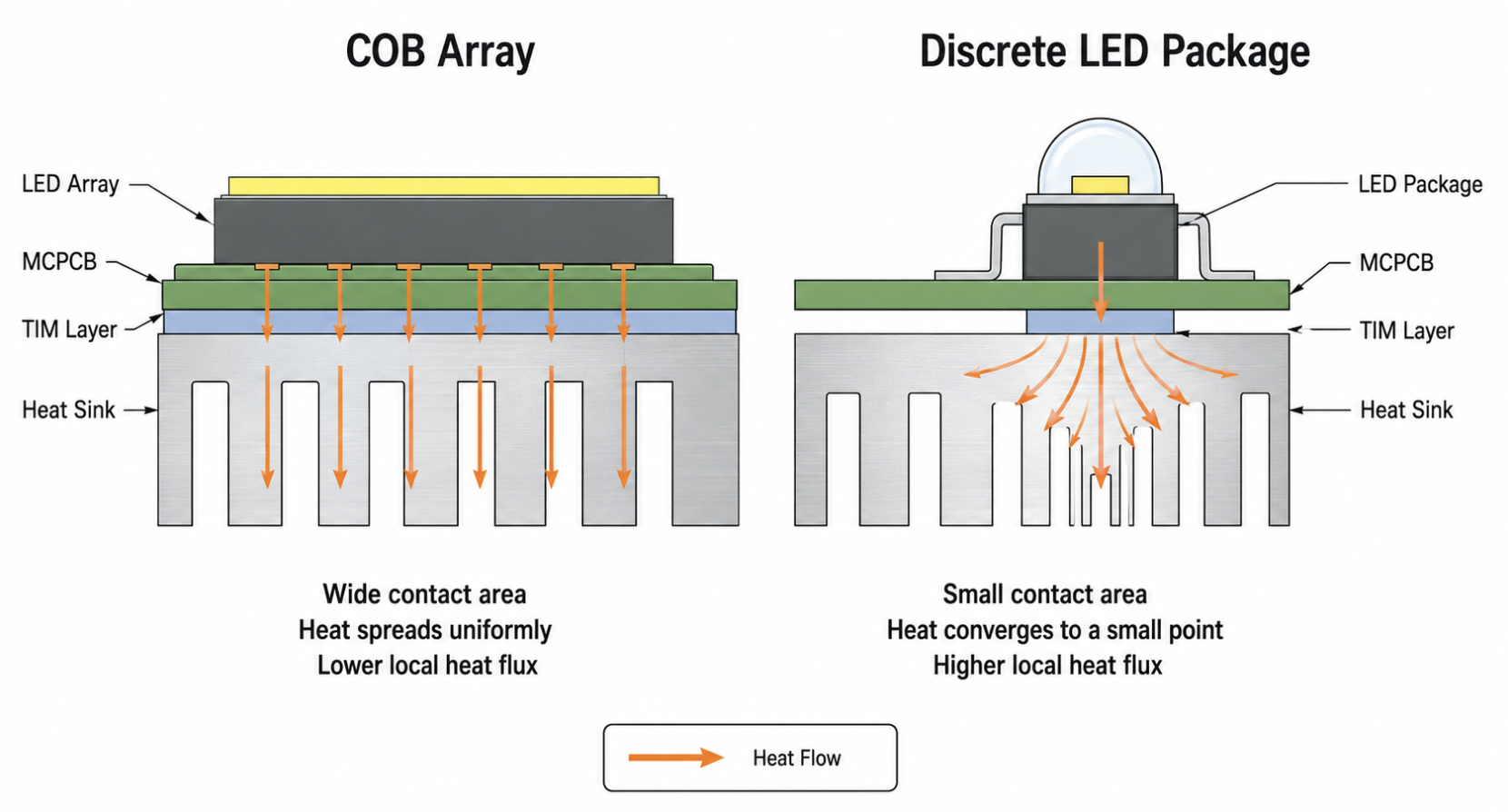
LED packages — particularly COB arrays and high-power discrete packages — typically present a single, well-defined contact area with concentrated heat flux, often significantly higher per unit area than individual driver components. A high-power COB array can dissipate tens of watts from a contact area of only a few square centimeters, producing heat flux considerably higher than a typical driver MOSFET dissipating similar total power over a larger PCB footprint. This concentration of heat flux at the LED interface is what drives the specific TIM requirements covered in the next section — requirements that differ meaningfully from the moderate, distributed heat loads typical of driver circuit components.
Key TIM Requirements for LED Packages
Thermal conductivity matched to heat flux, not just power level.
Because LED packages concentrate heat into a small contact area, the relevant design parameter is heat flux (W/cm²) rather than total power alone. A 50W COB array with a 4 cm² contact area presents roughly 12.5 W/cm² heat flux — a level that generally warrants TIM conductivity in the 3–6 W/m·K range at minimum, with higher-power or more compact arrays pushing toward 6–8 W/m·K to keep the TIM's contribution to total thermal resistance within an acceptable fraction of the overall budget.
Thin bond line thickness.
Given the concentrated heat flux at LED interfaces, bond line thickness has an outsized effect on junction temperature compared to many other TIM applications. Where a driver circuit component might tolerate a 1–2mm pad without significant thermal penalty, LED package interfaces benefit from BLT in the 0.1–0.5mm range where the contact geometry allows it — favoring PCM, thermal grease, or thin high-conductivity pads over standard-thickness pad formats.
Reliability tied directly to lumen maintenance.
TIM degradation at the LED interface does not just increase thermal resistance in the abstract — it directly accelerates lumen depreciation and shortens the L70/L90 rated lifetime of the fixture, because junction temperature and lumen maintenance are directly linked parameters in LED performance. This makes long-term TIM stability at this interface arguably more consequential than at driver circuit interfaces, where component failure — rather than gradual performance degradation — is typically the primary reliability concern.
Electrical insulation requirements depend on package type.
Some LED packages have an electrically isolated thermal pad on the package underside, in which case the TIM does not need to provide electrical insulation — the isolation is built into the package itself. Other package types, particularly some COB configurations, may have the LED die electrically connected to the thermal pad, in which case TIM electrical insulation is a hard requirement to prevent short circuits to a grounded heat sink or MCPCB. Verify the specific LED package's electrical isolation characteristics from the manufacturer's datasheet before assuming either configuration.
TIM Options for LED Chip-Level Interfaces
| TIM Type | Thermal Conductivity | Typical BLT | Best Fit Package Type | Key Consideration |
|---|---|---|---|---|
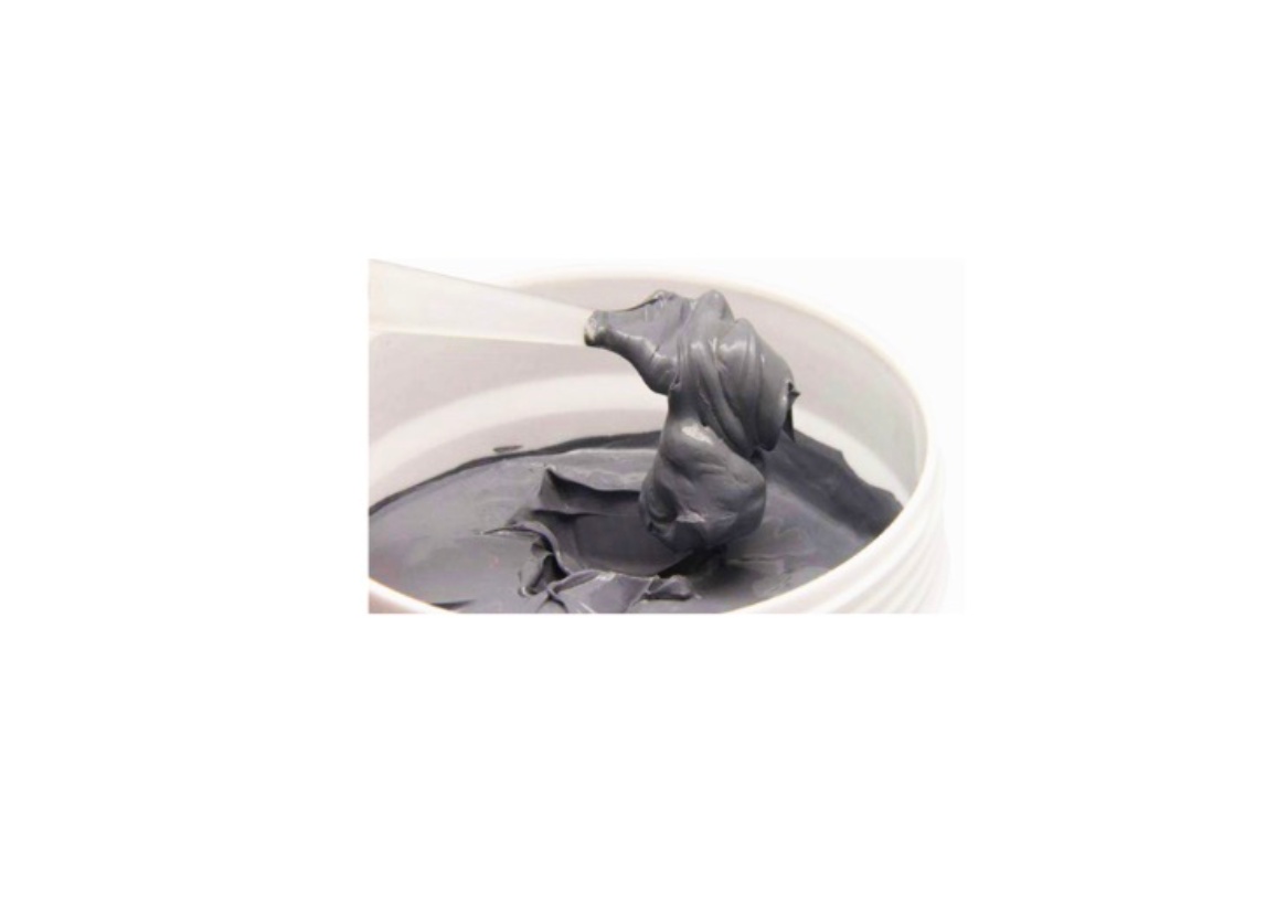
| Thermal grease | 3–10+ W/m·K | 20–100 µm | Discrete high-power LEDs, flat mating surfaces | Pump-out risk in long-life sealed fixtures |
| PCM | 3–8 W/m·K | 20–80 µm | COB arrays, discrete packages with flat contact | Requires activation temperature verification |
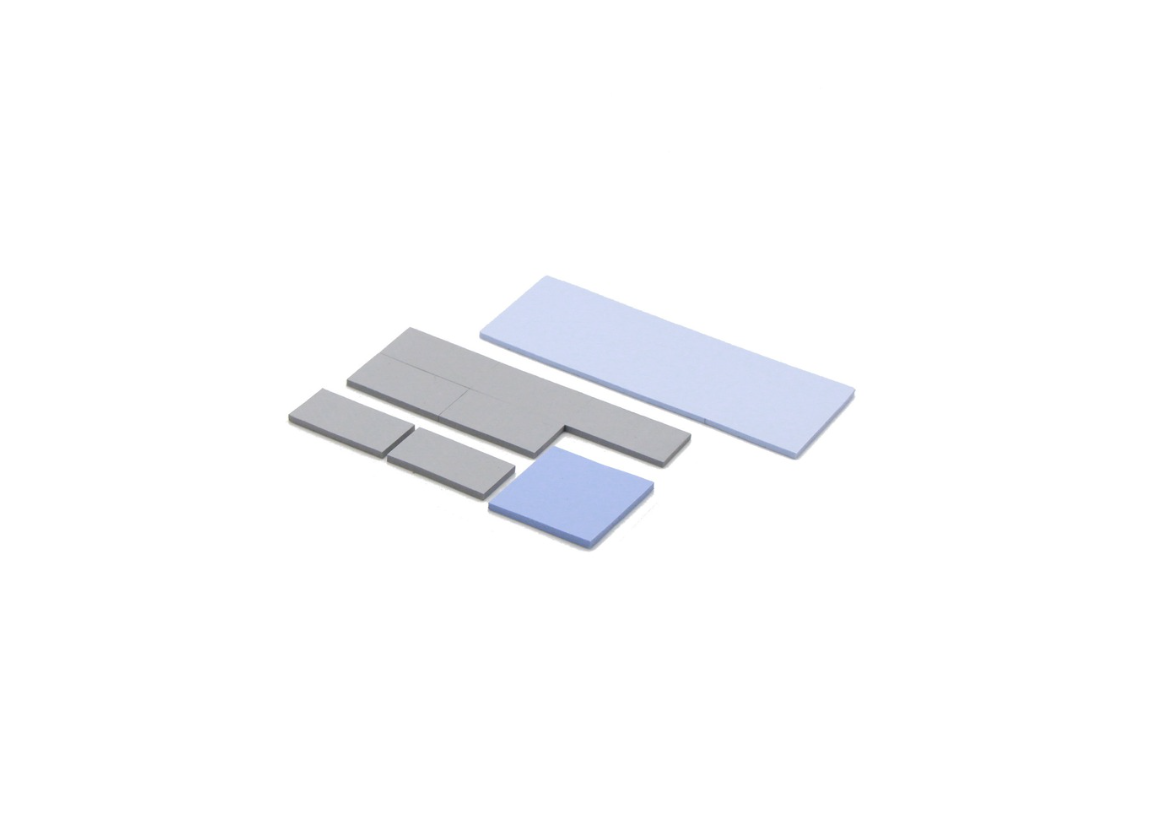
| Thin high-conductivity pad | 3–8 W/m·K | 0.1–0.5mm | COB arrays, MCPCB-mounted packages | Balances gap tolerance with thin BLT need |
| Graphite film | 3–10 (through-plane) / 300+ (in-plane) W/m·K | 0.05–0.2mm | Compact designs needing heat spreading | Not a substitute for interface contact material |
How to read this table for LED package selection:
Thermal grease and PCM both achieve the thin bond lines that concentrated LED heat flux favors, but their long-term reliability profile differs — grease is more prone to pump-out over a multi-year sealed fixture lifetime, while PCM offers better long-term stability provided the interface reliably reaches its activation temperature during operation. Thin high-conductivity pads offer a middle ground: less optimal BLT than grease or PCM, but simpler assembly and no activation temperature dependency.
Graphite film deserves a specific note: it is a heat spreader, not a primary interface material, for the same reasons covered in the PCM versus graphite comparison for power electronics. In LED applications, graphite is most useful as a secondary layer — spreading concentrated heat from a small LED contact area across a larger MCPCB or heat sink surface — used in combination with a proper interface material at the direct LED-to-substrate contact, not as a replacement for it.
COB vs. Discrete LED Package Considerations
COB (Chip-on-Board) arrays.
COB packages mount multiple LED die directly onto a substrate, creating a larger, flatter contact area than individual discrete LED packages — often several square centimeters compared to the much smaller footprint of a single discrete LED. This larger, flatter geometry generally favors pad or PCM formats, which perform well across broader contact areas and can accommodate the substrate's flatness tolerance more readily than materials optimized for very small, tightly controlled interfaces.
COB arrays also frequently mount directly to an MCPCB (metal-core PCB), which then interfaces to a separate heat sink — meaning there may be two TIM interfaces to consider in the full thermal path: LED-to-MCPCB (often handled by the COB substrate design itself) and MCPCB-to-heat-sink (a separate TIM selection decision, generally similar to standard PCB-to-heat-sink interfaces elsewhere in the fixture).
Discrete high-power LED packages.
Individual high-power LED packages present a smaller, more concentrated contact area — often just a few millimeters square for the thermal pad on the package underside — producing very high local heat flux despite comparatively modest total power dissipation. This concentration favors thermal grease or PCM over standard pad formats, since achieving adequate contact and thin BLT across a very small contact area is more consistently achievable with a conformable, thin-bond-line material than with a pre-formed pad that must be precisely sized and positioned.
Practical implication for mixed designs.
Many LED fixtures combine both package types — COB arrays for primary illumination alongside discrete LEDs for accent or secondary functions — which means a single fixture design may reasonably specify different TIM types at different LED locations based on package geometry, rather than defaulting to one material across the entire assembly.
Common Mistakes Specific to LED Chip-Level TIM
Applying driver circuit TIM logic to LED package interfaces.
A standard silicone thermal pad selected for a driver MOSFET — moderate conductivity, 0.5–1mm thickness, chosen primarily for ease of assembly — is frequently inadequate at the LED package interface, where the concentrated heat flux and thin-BLT requirement call for a fundamentally different material approach. Treating the LED interface as "just another thermal pad location" and defaulting to the same specification used elsewhere in the fixture is one of the most common sources of underperforming LED thermal designs.
Ignoring the manufacturer's junction-to-case thermal resistance data.
LED datasheets specify junction-to-case thermal resistance as a fixed parameter — this number, combined with your TIM and heat sink resistance, determines actual junction temperature at a given power level. Designing the TIM and heat sink without first pulling this value from the LED datasheet means the thermal budget calculation is incomplete, and there is no reliable way to verify whether the selected TIM provides adequate margin until the fixture is built and measured.
Overlooking the link between TIM degradation and lumen depreciation.
Because TIM performance directly affects junction temperature, and junction temperature directly affects lumen maintenance, TIM degradation at the LED interface produces gradual light output decline that is easy to misattribute to LED aging rather than interface degradation — a failure pattern similar to the siloxane contamination issue covered in other guides, but driven by a different mechanism (thermal resistance increase rather than optical surface contamination). Both point to the same underlying lesson: TIM reliability at the LED interface deserves the same qualification rigor as the LED component itself, not less.
Assuming graphite film alone solves an LED thermal problem.
Graphite's excellent in-plane conductivity makes it tempting to specify as a complete solution for LED hot spot management, but it does not eliminate the need for proper interface contact at the LED-to-substrate boundary. Specifying graphite in place of — rather than alongside — an appropriate primary interface material typically produces worse results than expected, because the fundamental contact resistance problem at the LED package boundary remains unaddressed.
TaxoTape® Solutions
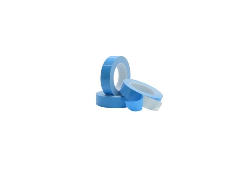
TaxoTape® supplies thermal grease, phase change materials, thin high-conductivity thermal pads, and graphite films suited to LED chip-level thermal interfaces — including COB array and discrete high-power LED package applications.
For COB and MCPCB-mounted LED designs, we can recommend appropriate conductivity grade and format based on your package contact geometry and heat flux. For discrete high-power LED applications requiring ultra-thin bond lines, PCM and grease options are available with full technical documentation including ASTM D5470 thermal resistance data and, where relevant, activation temperature specifications for PCM grades.
Request samples or technical consultation for LED thermal interface applications →
Conclusion
TIM selection at the LED package-to-heat-sink interface is governed by a different set of constraints than driver circuit TIM selection — concentrated heat flux, thin bond line requirements, and a direct, measurable link between interface degradation and lumen depreciation over the fixture's rated life.
Matching TIM type to LED package geometry — pad or PCM for COB arrays with their larger, flatter contact areas; grease or PCM for discrete packages with small, concentrated contact points; graphite as a complementary heat-spreading layer rather than a standalone solution — produces a more reliable thermal design than applying generic TIM selection logic borrowed from driver circuit or general power electronics applications.
Starting from the LED manufacturer's published junction-to-case thermal resistance, and building the TIM and heat sink specification around that fixed constraint, is the foundation for a thermal design that delivers the LED's rated lumen maintenance and service life in practice, not just on paper.
Contact TaxoTape® to discuss TIM selection for your LED chip-level thermal design →
FAQ
Q: Where do I find the junction-to-case thermal resistance value for my LED package?
This value is a standard parameter in LED manufacturer datasheets, typically listed as Rth(j-c) or similar notation, expressed in °C/W. It is specific to the exact LED package and mounting configuration — confirm you are using the value for your specific part number and package variant, since junction-to-case resistance can differ meaningfully between similar-looking packages from the same manufacturer's product line.
Q: Can I use the same TIM at both the LED package interface and the driver circuit interfaces in the same fixture?
Not always advisable. LED package interfaces typically benefit from thinner, higher-conductivity materials matched to concentrated heat flux, while driver circuit interfaces often have more forgiving thermal requirements but larger gap tolerances. Using a single TIM specification across both may result in over-specifying (and overpaying for) the driver interfaces, or under-specifying the LED interface. Evaluate each location's specific heat flux and gap geometry rather than defaulting to one material for the entire fixture.
Q: How much does TIM selection actually affect LED lumen maintenance in practice?
The relationship is indirect but measurable: TIM interface resistance is one contributor to total junction-to-ambient thermal resistance, and junction temperature is a direct input to the LED's rated lumen maintenance curve published by the manufacturer. A TIM that adds meaningfully more interface resistance than necessary — whether through poor material selection, degradation over time, or incorrect BLT — raises junction temperature correspondingly, which according to most LED manufacturers' published lumen maintenance data can shift the fixture's L70 or L90 rated lifetime by a substantial margin depending on how far above the optimal junction temperature range the design operates.
Q: Is PCM safe to use with LED packages given the activation temperature requirement?
Yes, provided the activation temperature is verified against your specific application's operating profile — the same consideration that applies to PCM in any application. Confirm that your LED package reliably reaches the PCM's phase transition temperature (commonly 45–65°C) during normal operation, not just at peak brightness or ambient extremes. If your fixture design keeps LED case temperature below the PCM's activation point during typical operation, the material will not deliver its intended performance and a different TIM type is more appropriate.